Flogen
2019 - Sustainable Industrial Processing Summit & Exhibition
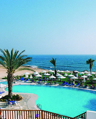
23-27 October 2019, Coral Beach Resort, Paphos, Cyprus
Abstract still accepted for a limited time
Almost 500 Abstracts Submitted from 60 Countries
Six Nobel Laureates have already confirmed their attendance: Profs. Dan Shechtman, Kurt Wüthrich, Ferid Murad, Rudy Marcus, Yuan Lee and Klaus Klitzing.
NEWS
Abstract Submission

DETAILLED PROGRAM OVERVIEW

Back
    Lanthanum Silicate for High-Dielectric Gate Insulator
    Hiroshi Iwai1;
    1TOKYO INSTITUTE OF TECHNOLOGY, Yokohama, Japan;
    PAPER: 80/SISAM/Invited (Oral)
    SCHEDULED: 17:50/Fri. 25 Oct. 2019/Dr. Christian Bernard


    ABSTRACT:
    Progress of microprocessors or logic integrated circuits has been conducted by the continuous miniaturization of Si MOSFETs. In the course of the miniaturization, the gate length and the gate oxide thickness have been reduced with the same ratio. Silicon dioxide (SiO<sub>2</sub>) has been used as the gate insulator for many years. In order to decrease the equivalent gate oxide thickness (EOT) to less than 1 nm, high-dielectric material is necessary [1] and hafnium dioxide (HfO<sub>2</sub>) [2] was chosen to replace SiO<sub>2</sub>. For further decreasing of the EOT to sub-0.5 nm, lanthanum oxide (La<sub>2</sub>O<sub>3</sub>) is supposed to be one of the best candidates among many materials when considering the band-offset and dielectric constant values [3]. Then, La silicate is expected to be even better because La silicate has some good properties similar to SiO<sub>2</sub>. In this paper, excellent MOSFET characteristics with 0.4 nm EOT gate oxide are demonstrated by introducing La silicate as the gate dielectrics. After the n<sup>+</sup> source and drain formation on the p-Si substrate, the La<sub>2</sub>O<sub>3 </sub>gate oxide film was deposited by an ultra-high vacuum evaporation method, followed by tungsten (W) and tantalum nitride (TaN) gate electrode film deposition by in situ RF sputtering under ultra-high vacuum conditions. After the gate electrode patterning, 3% forming gas annealing was performed for 30 minutes. After the annealing, a thin La silicate gate insulator was created with a smooth interface. The diffusion of oxygen into the gate oxide and the resulting increase of the EOT were almost completely suppressed by the combination of the stacked TaN and W gate electrode and the ambient forming gas during the annealing. The minimum EOT value obtained by C-V measurement was 0.4 nm. Very low values for the interface state density for the La silicate MOS capacitor of less than 10<sup>11</sup>cm<sup>-2</sup>eV<sup>-1</sup> were observed during the forming gas annealing performed above 850<sup>o</sup>C. The fixed charge density evaluated by the flat-band voltage was 1.0 X 10<sup>11</sup>cm<sup>-2</sup>. La silicate films are composed of good glass network structures as those of SiO<sub>2</sub> and have high viscosity at high temperatures. The movement of the atoms at a high temperature recovers the defects at the interfaces and in the films. This is the reason for the low interface state and fixed charge densities. Good I<sub>d</sub> - V<sub>d</sub> characteristics of a 0.4 nm EOT MOSFET were confirmed because of the excellent interfacial property. Due to the high band offset value between the conduction-bands of the Si channel and the La silicate gate insulator, the tunneling leakage current was almost completely suppressed down to EOT = 0.4 nm.

    References:
    [1] C. Fiegna, H. Iwai, T. Wada, T. Saito, E. Sangiorgi, B. Ricco, Dig. Tech. Symp. on VLSI Tech. (1993) 33-34.<br />[2] K. Mistry et al., IEDM Tech. Dig. (2007), 247 - 250.<br />[3] T. Hattori, T. Yoshida, T. Shiraishi, K. Takahashi, H. Nohira, S. Joumori, K. Nakajima, M. Suzuki, K. Kimura, I. Kashiwagi, C. Ohshima, S. Ohmi, H. Iwai, Microelectronic Engineering 72 (2004) 283 - 287.