Home
About
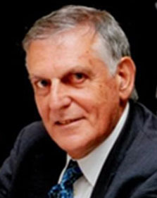
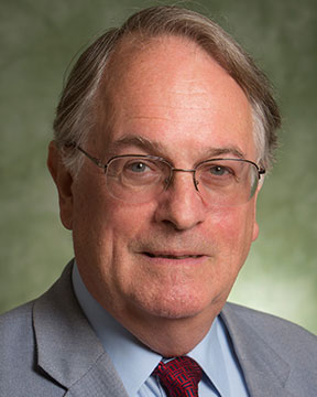
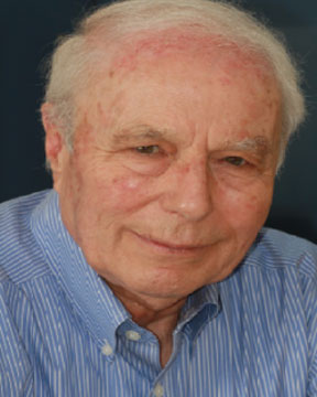
Prof. Stanley Whittingham
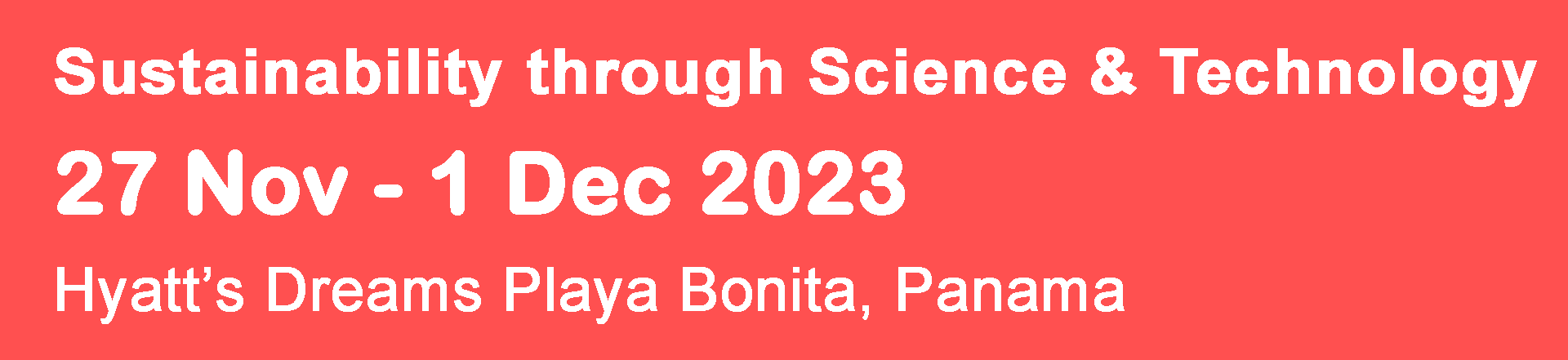
Summit
Organizers
Symposia
Leading Committee
Symposia Committees
Intl. Committees
Venue
Geographical Location
Meeting
Accommodation
On-Site Practical Info
Photos
Videos
Information
Announcements
Download logos
Download Banner
Download Flyer
Publications
Important Dates
Fees
Financial Support
Travel
Travel Insurance Policy
Visas
Invitation Letter
News
Sponsorship
Sponsors
Sponsorship Info
Exhibition Info
Submission
Login
Abstract
Paper
Program
General Program Grid
Detailed Program Grid
Distinguished Lectures
List of Abstracts
Summit Plenaries
Interactive Program
Interactive Program
Printed Program
SIPS 2023 ADDENDUM
Workshops
Social Program
Recreational Activities
Registration
Create an Account
Create an Account
Registration
Fees
Guidelines
Flow of Events
Types of Presentations
Abstract Preparation
Paper Preparation
Oral Presentation
Poster Presentation
Symposium (Co-)Chairs
Scheduling Guidelines for (Co-)Chairs
Session Chair
Session Monitor
Post Summit
Reports
Articles
Photos
Videos
Previous Summits
SIPS 2022
SIPS 2019
SIPS 2018
SIPS 2017
SIPS 2016
SIPS 2015
SIPS 2014
SIPS 2013
SIPS 2011
SIPS 2006
SIPS 2003-1
SIPS 2003-2
Videos
Nobel Laureates
Advanced Materials
CEO/Director/Entrepreneurship
Chemistry
Energy
Ferro-alloys
Geomechanics
Impressions
Intelligent Materials and Complex Systems
Iron and Steel Making
Laws and their Applications
Medicine
Mining
Molten Salts and Glass-forming Liquids
Multiscale Material Mechanics
Non-ferrous
Physics
Politics
Promotional Videos
Recycling
Contacts
Contact Us
Menu ☰
Close ☰
In Honor of Nobel Laureate Prof. M Stanley Whittingham
Abstract Submission Open
! About 500 abstracts submitted from around 60 countries.
Featuring many Nobel Laureates and other Distinguished Guests
Login
|
Registration
|
Hotel
| Personal Schedule
❮
❯
Back