2018 - Sustainable Industrial Processing Summit & Exhibition
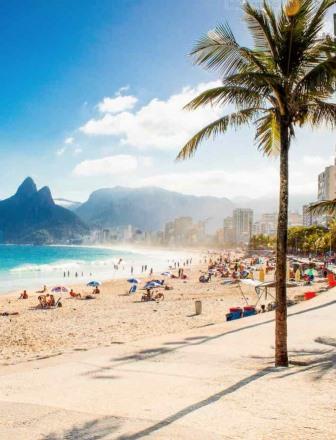
4-7 November 2018, Rio Othon Palace, Rio De Janeiro, Brazil
Seven Nobel Laureates have already confirmed their attendance: Prof. Dan Shechtman, Prof. Sir Fraser Stoddart, Prof. Andre Geim, Prof. Thomas Steitz, Prof. Ada Yonath, Prof. Kurt Wüthrich and Prof. Ferid Murad. More than 400 Abstracts Submitted from about 60 Countries.
Abstract Submission
Login

DETAILLED PROGRAM OVERVIEW

Back
    Applications of Chalcogenides: S, Se, and Te
    Gurinder Ahluwalia1;
    1COLLEGE OF THE NORTH ATLANTIC, Labrador City, Canada;
    PAPER: 164/AdvancedMaterials/Invited (Oral)
    SCHEDULED: 12:35/Wed./Grego (50/3rd)


    ABSTRACT:
    The changing landscape of research, from pure scientific ventures towards industrial applications, necessitates investigation of novel materials for several applications. In the present work, I will discuss various aspects of research on materials for industrial applications, with emphasis on use of chalcogenides for optical fibers, electrochemical sensing, imaging and detection, biochemical sensing, data storage, photovoltaics and infrared detection. The peculiar properties of chalcogenides arise due to the lone pair orbitals forming the valence band as a result of their electronic configuration. At the same time, dangling bonds play an important role to modify the electrical behavior of chalcogens in amorphous forms. In particular Sulfur (S), Selenium (Se) and Tellurium (Te) find applications in a variety of devices used in the electronics and optoelectronics industry. Sulfur based materials exhibit interesting properties such as a high refractive index, large Kerr non-linearities, ability to be directly patterned by exposure to near band gap light, good transmission in the IR beyond 1.5m. Selenium based materials find wide applications in rectifiers, solar cells, photographic exposure meters, xerography and anticancer agents. It is also used in the glass industry to eliminate bubbles and remove undesirable tints produced by iron. In addition, selenium also has a high reactivity towards a wealth of chemicals that can be potentially exploited to convert selenium into other functional materials such as CdSe, ZnSe, Ag2Se and so on. Selenium based materials in amorphous form are used for imaging and biomedical applications. In crystalline form, their combination with other materials such as lead (Pb), Copper (Cu) and Indium (In) are widely used for photovoltaic and photo-detection applications. Se and Te are lone pair, polymeric divalent materials with chain structures. They can be designed to bond with cross-linking elements of different bond strengths such as Ge, Sb and As. The cross linked Te/Se alloys have a huge number of non-bonded lone pair electrons which could easily be excited by optical and electrical fields. When the amorphous phase cannot contain the excitation energy, a phase change to a crystalline phase occurs. Such polymeric lone pair structures are vibronic in nature wherein electronic transitions are made possible by vibrational motion of the chains. These simultaneous vibrational and electronic transitions form the basis of optical and electrical phase change memories. Tellurium based materials are widely used for data storage devices based on phase change characteristics exhibited by them. Applications such as optical fibers for communication and sensing, X-ray imaging, electrochemical sensors, data storage devices, biomedical applications, photovoltaics and IR detectors will be presented and the future scope and expected improvements to existing technologies will be discussed depending on the availability of time.

    References:
    [1] Applications of Chalcogenides: S, Se and Te. Ed Gurinder Kaur Ahluwalia, Springer 2017